Author: Olzhas S. Tazabekov (LinkedIn)
Prerequisites: basic programming skills with Python and SPICE
Intro
This is the second tutorial of the series dedicated to IC modelling with PySpice. Or how to not spend tons of money on CAD licenses for those half starving tech startups, so that the board members could keep their kidneys 😉 This tutorial will continue the discussion of modelling data converters and their components and will describe how to model an Analog-to-Digital Converter (ADC). Some of the DAC code and concepts covered in the previous article will be used here as well.
Ideal ADC
As was mentioned earlier, ideal models that consist of behavioural elements allow to analyze the performance of a mixed-signal circuit block within a reasonable amount of time. For example, if one has designed a DAC at the transistor level and want to simulate its operation under various temperatures and matching conditions, the one might want to apply a digital input code generated from an ideal ADC with a sine wave. The same way, if one has a digital signal processing system (DSP) and want to get an analog waveform output at any point where there is a digital word, the one can quickly drop an ideal DAC. (see Fig. 1)

Fig. 1. Digital Control System with Analog IO
An ideal ADC converts an input analog voltage or current to a certain number of bits N proportional to the magnitude of the voltage or current. The sequence of bits represents a digital number and each bit has a double of the weight of the next one, starting from the most significant bit (MSB) to the less significant one (LSB).
![\[ V_{in}=\sum_{n=0}^{N-1} b_n 2^n \dfrac{V_{ref}}{2^N} \]](http://www.tazabekov.com/blog/wp-content/ql-cache/quicklatex.com-85a81012e47f352b9f5a5b721cb7f1fc_l3.png "Rendered by QuickLaTeX.com")
So, the MSB has weight of Vref/2, the next one has weight of Vref/4, etc. Finally, the LSB has a weight of Vref/2^N.
The conventional implementation of the ideal ADC consists of an ideal Sample-and-Hold (S/H) followed by passing the output of the S/H (the held signal) through an algorithm to generate the output digital bits.
The following implementation is based on a pipeline ADC:
- The input signal is sampled and held,
- The held signal is fed into a comparator that compares the input value to the reference voltage,
- if the input signal is greater then the reference voltage, the output bit is set to high, and the reference signal is subtracted from the input. The difference is multiplied by two and passed to the output stage,
- If the input signal is less then the reference voltage, the output bit is set to low. The input signal is then multiplied by two and passed to the output stage,
- This output is used at the input to the next stage and steps 2, 3, and 4 above are repeated. This continues for N stages (where N is the number of bits in the ADC)
The common voltage Vcm can be determined by calculating the mid point between Vref+ and Vref- followed by subtracting Vref- so that Vcm is referenced around 0V.
![\[ V_{CM}=\dfrac{V_{REF+}+V_{REF-}}{2}, \]](http://www.tazabekov.com/blog/wp-content/ql-cache/quicklatex.com-7379c04a2c21cc786c0b41096d813499_l3.png "Rendered by QuickLaTeX.com")
![\[ V_{CM0}=\dfrac{V_{REF+}+V_{REF-}}{2}-V_{REF-}=\dfrac{V_{REF+}-V_{REF-}}{2}; \]](http://www.tazabekov.com/blog/wp-content/ql-cache/quicklatex.com-d6f5e331563ffcdd6aeffa8220711459_l3.png "Rendered by QuickLaTeX.com")
One might also want to level shift the input signal so that it is referenced to 0V and the transfer curves to the left by 1/2 LSB. The value of 1/2 LSB is given by:
![\[ 1/2 LSB =\dfrac{V_{REF+}-V_{REF-}}{2^{N+1}} \]](http://www.tazabekov.com/blog/wp-content/ql-cache/quicklatex.com-e61a960bd4a457764393a2fe5998a227_l3.png "Rendered by QuickLaTeX.com")
assuming Vref+>Vref- and N is the number of bits in the ADC. Again, level shifting the input and the common-mode voltage makes sense in order to make the model as flexible as possible (things are much simpler if Vref+ = VDD and Vref- = GND)
PySpice Modelling Approach
As was mentioned before, in order to implement an ideal ADC one needs to build the following sub blocks: sample-and-hold, level shifter and the pipeline stages.
Ideal Sample-and-Hold Circuit
The block diagram for an ideal S/H is shown below.The inputs are clock, Vin and the trip voltage, while the output is labeled as Vout.
Ideal Sample and Holde Subcircuit

          vdd
           |
         --------------------------------------------------------------------------
        |     -----------                                           ------------   |
    in--|    |           |                                         |            |  |
        |    |  -------  |                                         |  --------  |  |
   clk--|     -|-      | |                                          -|-       | |  |
        |      | inbuf |----inbuf--\ ---inS-------\ ---outS------|   | outbuf |----|--out
  trip--|  in--|+      |           |        |     |         |    |---|+       |    |
        |       -------            |      |Cap|   |       |Cap|       --------     |
        |                         clk_      |    clk        |                      |
        |                                   vss             vss                    |
         --------------------------------------------------------------------------
           |
          vss
Note, that both switches controlled by clk and clk_ can be closed momentarily at the same time for a period, which is approximately equal to one transient step. The charge sharing between the capacitors is affected by that, hence, the reasonably large ratio should be picked for the values (around 120 dB, i.e. a million-to-one). However, the shorter the time of both switches being closed, the smaller the ratio could be picked without affecting the circuit operation. Also note, that over a time set by GMIN (remember a resistor with a value of 1/GMIN is placed across every pn-junction in a SPICE simulation and GMIN default value is around 1E-12) and the capacitor values the charge on the capacitors will leak off causing a voltage drop. For example, for 0.1fF capacitor the associated RC time because of GMIN becomes 100us (increasing the capacitor to 10fF won’t affect the sampling operation and pushes RC time constant up to 10ms).
As one may see, the accuracy of the S/H is ultimately limited by the simulator tolerances (e.g. RELTOL, ABSTOL and VNTOL). However, this is not the topic of this tutorial and will be discussed later in more detail.
We now have to define a class for S/H, which incorporates a model for the switches, ideal caps and voltage controlled voltage sources acting as ideal voltage buffers. The code is given below
class IdealSampleHold(SubCircuitFactory):
    __name__ = 'IDEALSAMPLEHOLD'
    __nodes__ = ('in', 'trip', 'clk', 'vdd', 'vss', 'out')
    def __init__(self, **kwargs):
        super().__init__()
        #switches model
        self.swmod_params = {'ron':1E-3, 'roff':1E9}
        self.model('swmod','sw', **self.swmod_params)

        #элементы схемотехники Сэмпл Холд
        self.VCVS('in', 'in', 'inbuf', 'inbuf', 'vss', voltage_gain=100E6)
        self.VCS('1', 'trip', 'clk', 'inbuf', 'inS', model='swmod')
        self.C('s1', 'inS', 'vss', 1E-6)
        self.VCS('2', 'clk', 'trip', 'inS', 'outS', model='swmod')
        self.C('outS', 'outS', 'vss', 1E-8)
        self.VCVS('out', 'outS', 'out', 'out', 'vss', voltage_gain=100E6)
Ideal Pipeline Stage
Along with the supply rails the inputs for the following implementation of a pipeline stage block are input signal (‘in’), reference voltage (‘cm’), trip voltage for the switches (‘trip’). The outputs are the result output signal (‘out’) and the bit value (‘bitout’).
As was mentioned earlier, each stage compares an input signal with the reference voltage and assigns corresponding values to the bit output. Depending on the result of the comparison the stage then passes either a value of the input signal or its difference with Vref multiplied by two to the next stage.
The following code implements the ideal pipeline stage
class IdealPipelineStage(SubCircuitFactory):
    __name__ = 'IDEALPIPELINESTAGE'
    __nodes__ = ('in', 'cm', 'trip','vdd', 'vss', 'bitout', 'out')
    def __init__(self, **kwargs):
        super().__init__()
        #Swiches models
        self.swmod_params = {'ron':1E-3, 'roff':1E9}
        self.model('swmod','sw', **self.swmod_params)
        #Элементы схемотехники Пайплайн Стейдж
        self.VCS('1', 'in', 'cm', 'vdd', 'bitout', model='swmod')
        self.VCS('2', 'cm', 'in', 'vss', 'bitout', model='swmod')
        self.VCVS('outh', 'in', 'cm', 'vinh', 'vss', voltage_gain=2)
        self.VCVS('outl', 'in', 'vss', 'vinl', 'vss', voltage_gain=2)
        self.VCS('3', 'bitout', 'trip', 'vinh', 'out', model='swmod')
        self.VCS('4', 'trip', 'bitout', 'vinl', 'out', model='swmod')
N-bit Analog-to-Digital Converter
Now we have all the main blocks required to build a model for an ADC. The following implementation has positive/negative reference, clock and input signals as inputs along with the supply rails. The outputs are the digital bits for the corresponding number. The diagram is shown below. As was mentioned earlier, the the value of the input signal gets sampled by the S/H circuit and level shifted by LSB/2 value. The result then gets through the N number of pipeline stages producing corresponding digital bits.
Ideal ADC Subcircuit

            vdd
             |
           -------------------------------------------------------------------------------------------------------------------------
          |                                                                                                                         |
    refp--|-|                                                                                                                       |--bitout1
          | cm-----                    refp---    refn---                      --bitout1        --bitout2             --bitoutN     |
    refn--|-|      |                          |          |                    |                |                     |              |--bitout2
          |     |Sample/Hold|--outsh--|levelshift by lsb/2 & refn|--pipin--|stage1|--out1--|stage2|--out2-- ..N ..|stageN|--outN    |
     clk--|--------|   |                                                                                                            |-- ...
          |            |                                                                                                            |
      in--|------------                                                                                                             |--bitoutN
          |                                                                                                                         |
           -------------------------------------------------------------------------------------------------------------------------
             |
            vss
The following code implements an ideal model of the N-bit pipeline ADC.
class IdealAdc(SubCircuitFactory):
    __name__ = 'IDEALADC'
    def __init__(self, nbits, **kwargs):
        #number of bits
        self.nbits = nbits
        self.__nodes__ = ('refp', 'refn', 'vdd', 'vss', 'in', 'clk') + tuple([('b'+str(i)) for i in range(self.nbits)])
        super().__init__()
        #common voltage definition = (refp+refn)/2
        self.BehavioralSource('cm', 'cm', self.gnd, voltage_expression='(v(refp)+v(refn))/2')
        #logic switching point
        self.R('top', 'vdd', 'trip', 10E6)
        self.R('bot', 'trip', 'vss', 10E6)
        #ideal sample and hold
        self.X('idealsamplehold', 'IDEALSAMPLEHOLD', 'in', 'trip', 'clk', 'vdd', 'vss', 'outsh')
        #levelshift by refn and 1/2LSB
        self.BehavioralSource('pip', 'pipin', 'vss', voltage_expression='v(outsh)-v(refn)+((v(refp)-v(refn))/2^'+str(self.nbits+1)+')')
        #Каскад пайплайн стейдж
        self.X('idealpipelinestage'+str(self.nbits-1), 'IDEALPIPELINESTAGE', 'pipin', 'cm', 'trip', 'vdd', 'vss', 'b'+str(self.nbits-1), 'out'+str(self.nbits-1))
        for i in range(self.nbits-1, 0, -1):
            bitstr = str(i)
            prev_bitstr = str(i-1)
            self.X('idealpipelinestage'+prev_bitstr, 'IDEALPIPELINESTAGE', 'out'+bitstr, 'cm', 'trip', 'vdd', 'vss', 'b'+prev_bitstr, 'out'+prev_bitstr)
ADC/DAC Characterization Test Bench
It is important to realize the usefulness of the simulation model we have just developed. Should there be any analog/mixed signal simulation (using SPICE) or general system level simulation (using Matlab or Python), one can use the ADC model to degenerate a digital signal as an input source. The one can also use the developed earlier DAC model to convert a digital word into an analog waveform, which can be used for a block characterization or figuring out some system level parameters.
For the first test bench lets have a an ideal ADC developed in this tutorial and an ideal DAC developed in the previous tutorial. The ADC will be clocked at 100 MHz and have an analog input. The digital word generated by the ADC will be driving the DAC, which will generate an analog waveform. The diagram of the test bench is below.
                 ---        ---
                |   |--b0--|   |
      |in|--in--|ADC|--..--|DAC|--out
           clk--|   |--bn--|   |
                 ---        ---
Let’s begin by simply applying a ramp from Vref- to Vref+ to the input and use 3 bit ADC and DAC. The code is given below.
    #ADC/DAC Transient Test Bench Vars
    dac_nbits = 3
    adc_nbits = 3
    f_signal = 10E6
    amp_signal = 0.5
    dc_signal = 0.5
    f_sample = 100E6
    t_sample = 1/f_sample
    #Simulator Vars
    tran_sim_end_time = 1E2/f_signal

    #Ramp-up Test Bench Definition
    circuit_pwl = Circuit('TestBench')
    circuit_pwl.subcircuit(IdealDac(nbits=dac_nbits))
    circuit_pwl.subcircuit(BitLogic())
    circuit_pwl.subcircuit(IdealSampleHold())
    circuit_pwl.subcircuit(IdealPipelineStage())
    circuit_pwl.subcircuit(IdealAdc(nbits=adc_nbits))
    #Instantiating Sources
    # -input source
    circuit_pwl.V('in1', 'in1', circuit.gnd, 'pwl(0 0 '+str(tran_sim_end_time)+' 1 r=0')
    # -supply rails and references
    circuit_pwl.V('vdd', 'vdd', circuit.gnd, 1)
    circuit_pwl.V('refp', 'vrefp', circuit.gnd, 1)
    circuit_pwl.V('refn', 'vrefn', circuit.gnd, 0)
    # - clock
    circuit_pwl.Pulse('clk', 'clk', circuit.gnd, 0, 1, t_sample/2, t_sample, fall_time=0.01*t_sample, rise_time=0.01*t_sample)
    # -ADC/DAC
    circuit_pwl.X('ADC', 'IDEALADC', 'vrefp', 'vrefn', 'vdd', circuit.gnd, 'in1', 'clk', ', '.join([('b'+str(i)) for i in range(adc_nbits)]))
    circuit_pwl.X('DAC', 'IDEALDAC', 'vrefp', 'vrefn', 'vdd', circuit.gnd, ', '.join([('b'+str(i)) for i in range(dac_nbits)]), 'out')
    #Transient Sims
    # -instantiating a simulator
    simulator_pwl = circuit_pwl.simulator(temperature=25, nominal_temperature=25)
    # -defining Simulator Properties
    simulator_pwl.options('MAXORD=5')
    simulator_pwl.options('METHOD=Gear')
    # -Extractin Analysis Data
    analysis_pwl = simulator_pwl.transient(step_time=1E-9, end_time=tran_sim_end_time)
    #Printing the Circuit Nodes (optional)
    #print(analysis.nodes.values())

    #Plotting Transient Sims Data
    f, axarr = plt.subplots(adc_nbits+2, sharex=True)
    f.tight_layout()
    axarr[0].set_title('ADC Input and DAC Output')
    axarr[0].plot(analysis_pwl.time, np.array(analysis_pwl.in1))
    axarr[0].plot(analysis_pwl.time, np.array(analysis_pwl.out))
    axarr[1].set_title('ADC Clock and Trip Voltage')
    axarr[1].plot(analysis_pwl.time, np.array(analysis_pwl.clk))
    axarr[1].plot(analysis_pwl.time, np.array(analysis_pwl.nodes['xadc.trip']))
    for i in range(adc_nbits):
        axarr[i+2].set_title('ADC Bit '+str(i))
        axarr[i+2].plot(analysis_pwl.time, np.array(analysis_pwl.nodes['b'+str(i)]))
    axarr[len(axarr)-1].set_xlabel('time [s]')
    plt.show()
One can see how the digital bits of the ADC change according to the rising input voltage (000 corresponds to the lowest input voltage and 111 is for the highest one). Then the bits of the digital word control the DAC. Looking at the DAC output one can also see the LSB value of the system, which in this case is 0.125V.
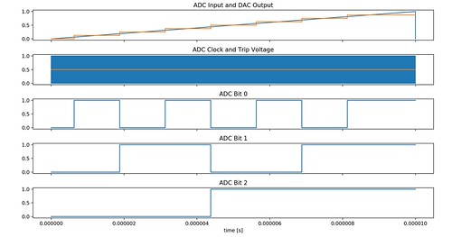
Fig. 2. Transient Analysis. Input Voltage Ramp-up
Viewing the ADC Quantization Noise Spectrum
At this point one should understand the sampling process and the operation of ideal ADC and DAC. Another useful thing is to explore a quantization noise (the effective noise added to a signal after passing through an ADC) and how it affects the spectrum of the signal.
Let’s consider a similar test bench but this time use 6-bit ADC and DAC and use a 10MHz sine wave as an input signal, which would swing from Vref- to Vref+. Minor modifications to the previous test bench are needed (change the bits and replace the input voltage source).
    #Instantiating Sources
    # -input source
    circuit.Sinusoidal('in1', 'in1', circuit.gnd, dc_offset=dc_signal, offset=dc_signal, amplitude=amp_signal, frequency=f_signal, delay=0, damping_factor=0)
This is what the plots look like.
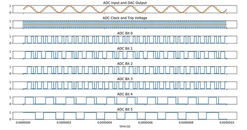
Fig. 3. Transient Analysis. Sampling a Sine Wave
Now, this quantization is not obvious after looking at the time domain response. However, looking at the spectrum of the ADC input and the DAC output should reveal the difference in the noise floor between the two. Transforming the signals from time to frequency domain can be done using FFT methods from Python libraries.
    #Quantization Noise. Fourier Transform of the ADC input and DAC Output
    N = np.array(analysis.in1).size
    T = analysis.time[1]-analysis.time[0]
    print('N: '+str(N))
    print('T: '+str(T))
    signal = np.array(analysis.in1)
    fft_signal = np.abs(np.fft.fft(signal))
    max_fft_signal = np.max(fft_signal)
    output = np.array(analysis.out)
    fft_output = np.abs(np.fft.fft(output))
    max_fft_output = np.max(fft_output)
    freq_fft = np.linspace(0, 1/(2*T), N//2)
    f_q, axarr_q = plt.subplots(2)
    f_q.tight_layout()
    axarr_q[0].set_title('ADC Input and DAC Output Noise Floor. Frequency Domain ')
    axarr_q[0].plot(freq_fft[:N//2], 20*np.log10(2/N*fft_signal[:N//2]))
    axarr_q[0].plot(freq_fft[:N//2], 20*np.log10(2/N*fft_output[:N//2]))
    axarr_q[1].set_title('ADC Input and DAC Output. Time Domain')
    axarr_q[1].plot(analysis.time, signal)
    axarr_q[1].plot(analysis.time, output)
    plt.grid(True)
    plt.show()
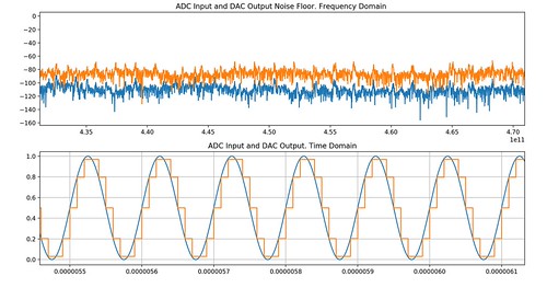
Fig. 4. ADC Input and DAC Output in Time and Frequency Domains
As it can be seen from the plots, the noise floors are different. The noise floor associated with the DAC output is related to the RMS quantization noise voltage, which can be found as
![\[ V_{Q_e,RMS}=\sqrt{ \frac{1}{T} \int_0^T (0.5 LSB -\frac{1 LSB}{T}*t)^2 \mathrm{d}t = \frac{V_{LSB}}{\sqrt{12}}} \]](http://www.tazabekov.com/blog/wp-content/ql-cache/quicklatex.com-1c130e1fd725be9be3a926c778770dfa_l3.png "Rendered by QuickLaTeX.com")
For example, for a case of an 8-bit ADC with 1 V range where 1LSB=3.9mV, Vqrms=1.1mV or -59dB. And the higher the bit number, the closer the quantized noise floor gets to the noise floor of the input signal. For a 12-bit ADC, Vqrmr=70.5uV or -83dB.
Conclusions
This tutorial explains how to model an analog to digital converter with PySpice. Some basic theory of the sampling process and the operation of an ideal ADC and a DAC was covered. Python classes implementing Ideal blocks for pipeline ADC (e.g. S/H and pipeline stage) and the N-bit ADC itself were built. Some examples of basic test benches for transient analysis were shown. It was also shown how to extract the data and post-process it with Python FFT packages for quantization noise analysis.
General References
- GitHub Repository with the complete code for this tutorial: https://github.com/OlzhasT/PySpiceCircuits-/blob/master/adc_dac_ideal_subcircuit_class_test.py,
- Previous part (Part 1) of this tutorial series: Digital to Analog Converter Modelling with PySpice,
- All the PySpice documentation and installation guidelines: https://pypi.python.org/pypi/PySpice/0.3.3,
- PySpice examples explaining how to get started with simple circuits and basic analysis and data processing: https://pyspice.fabrice-salvaire.fr/examples/index.html;